FPGA DESIGN OVERVIEW
The role of the UPduino v3.1 FPGA in this project is to generate a signal that simulates the output of a current passing through an insect. By using a MCP4822 12-bit DAC, it is possible to send data values to the DAC, and get a clean analog signal. The DAC uses an SPI communication protocol, which allows for faster data transmission than other communication protocols such as UART.
The FPGA was programmed using an FSM that determines whether to send a new data value, or whether to keep the DAC IDLE. With the on-board 48 MHz oscillator, it is possible to divide to a 3 MHz clock which was used for the SPI clock (SCK) as well as divide to a much lower frequency clock to determine a new data value from a big look-up table.
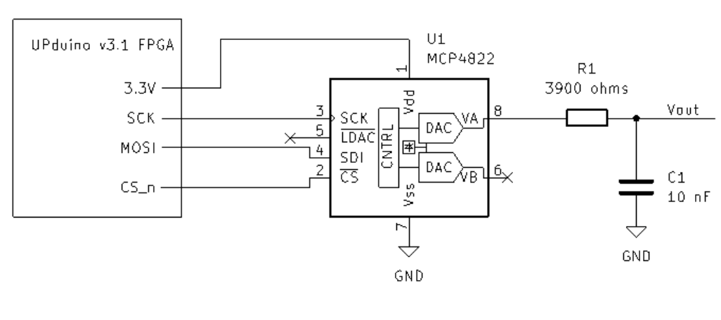
FPGA block diagram overview
The output of the DAC goes to a reconstruction filter that smooths out the high frequencies, cleaning the signal further. From there, the output signal goes straight into the ADC of the Nordic MCU.
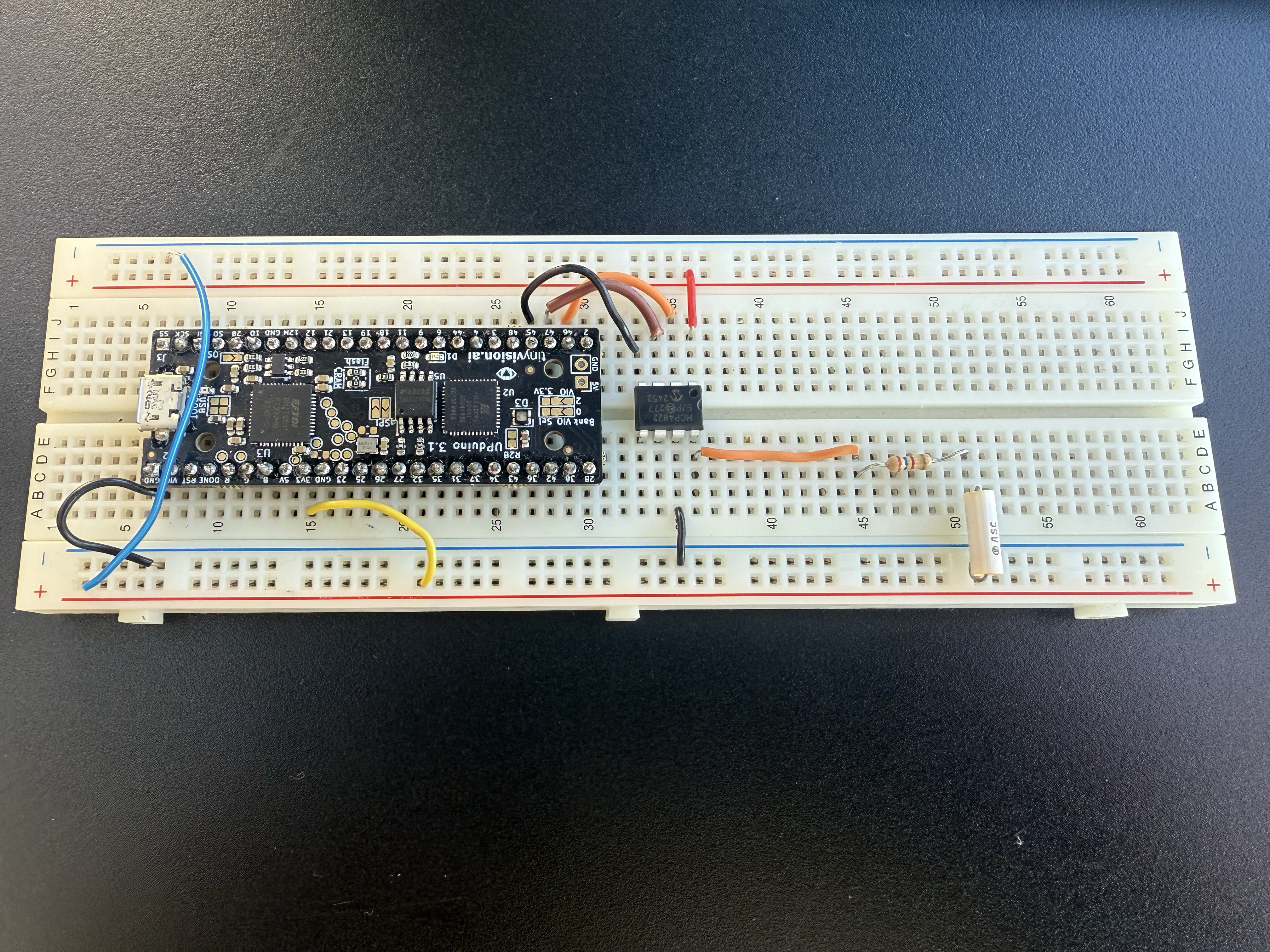
FPGA circuit on breadboard
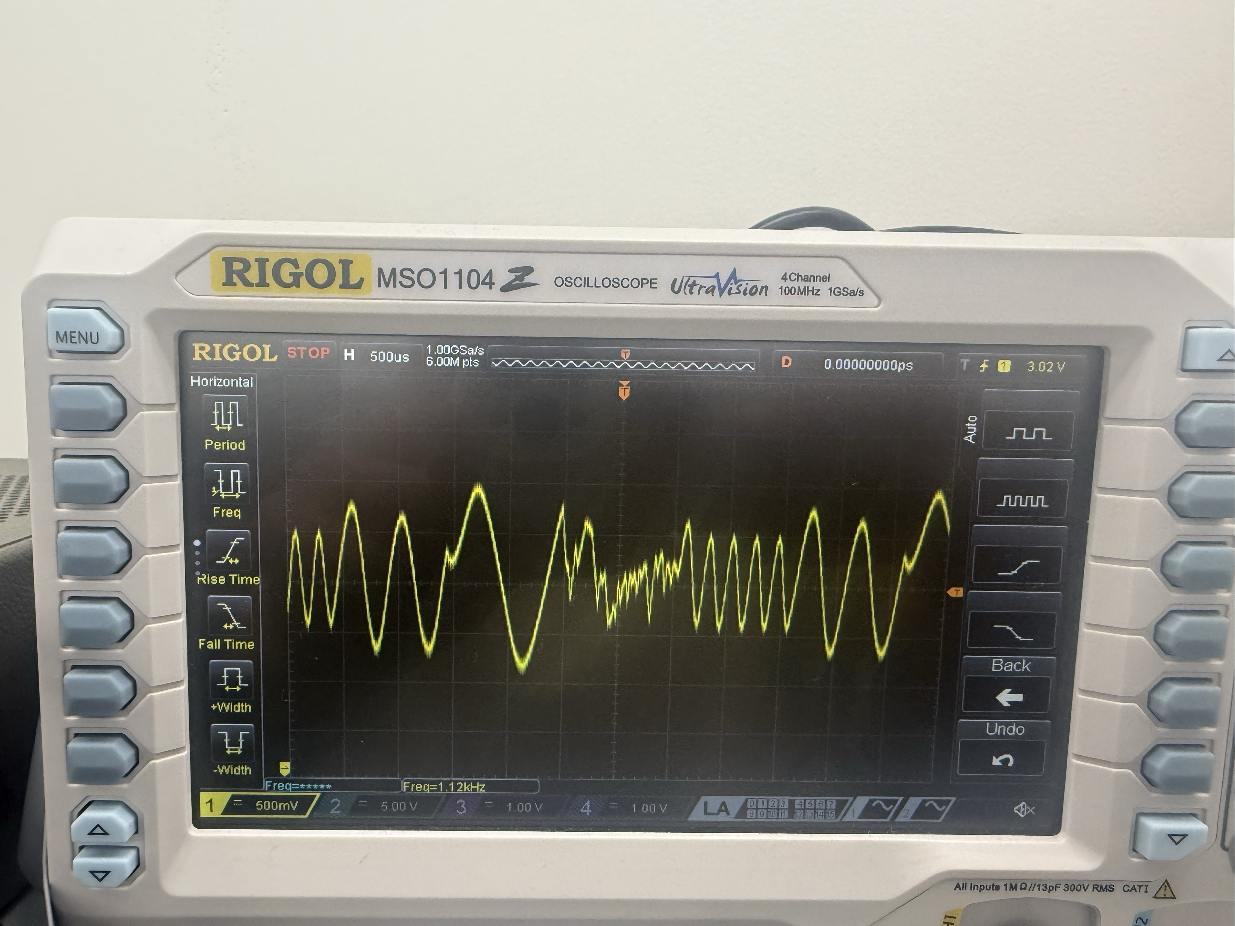
Below is the signal that is generated from the FPGA as can be seen from the oscilloscope of a sine wave with frequency of 1 kHz.
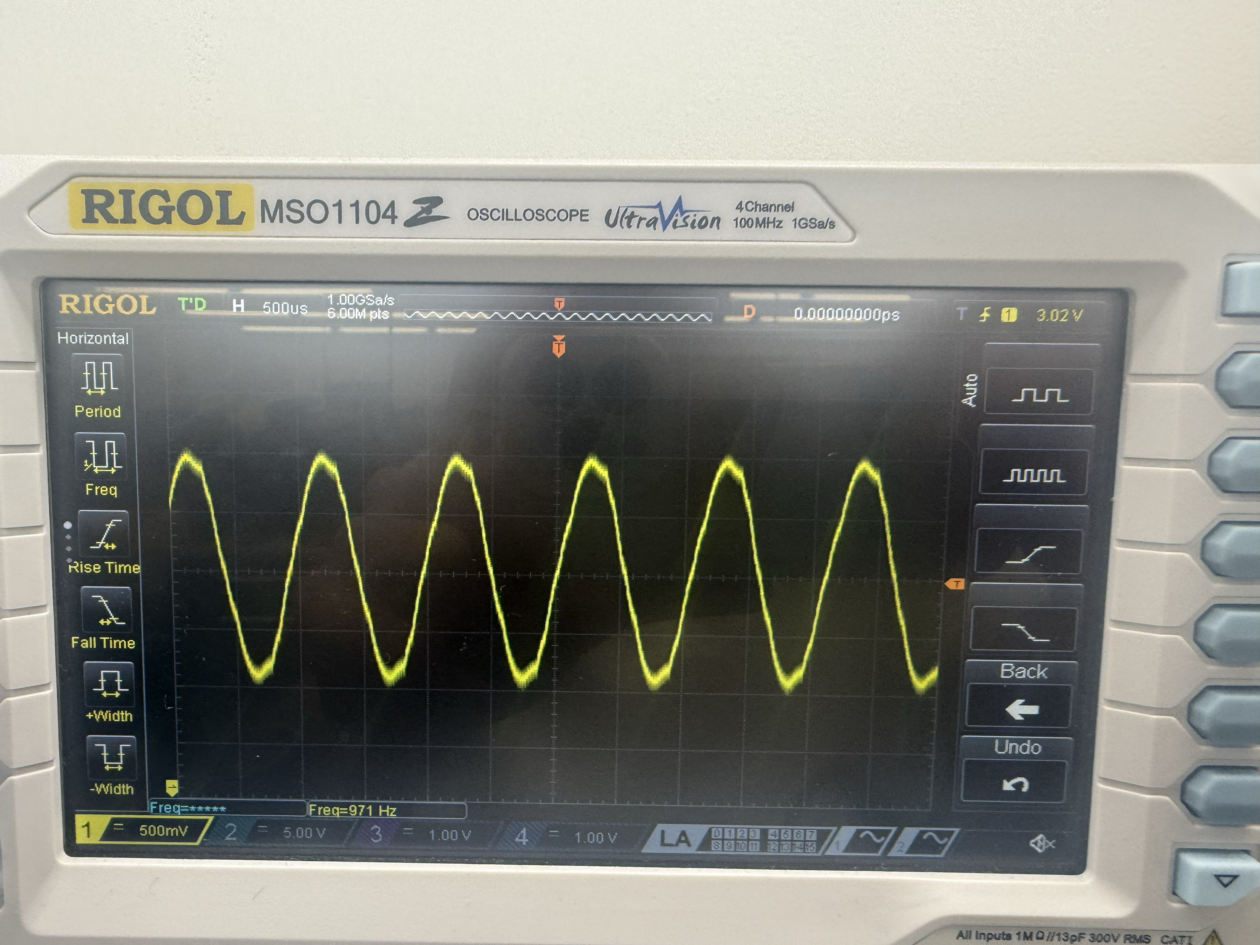
Trace of Sine wave (1kHz)
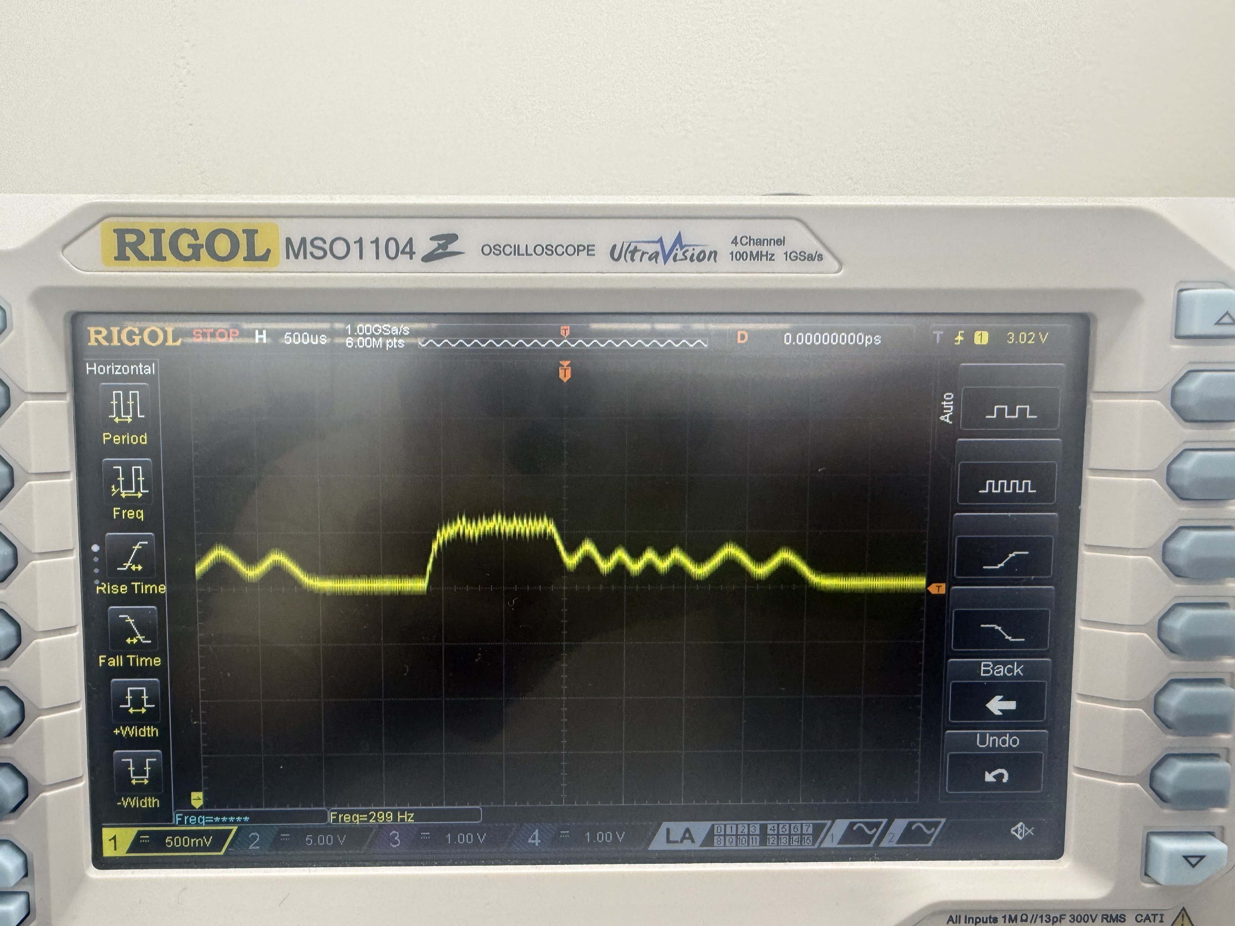
We also added another signal that matched a little closer what the output of an insect would look like to get accurate results. These included an alternating frequency signal and a signal that matched the output signal of an insect after current is applied to it.