Bill of Materials:
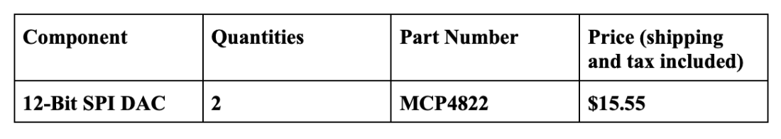
Bill of Materials
New Hardware:
The design uses the MCP4822, which is a dual 12-bit digital to analog converter that provides two precise voltage outputs. It communicates over an SPI interface, allowing our FPGA to generate accurate analog signals. Each channel supports rail-to-rail output and includes a gain amplifier that can be programmed. The chip select (CS_n) inside of the DAC is active low and LDAC is active low as well. The LDAC updates the data immediately when it is tied low, and if it is held high, no new data value will be updated.
The FPGA uses shifters to update the value of MOSI, sending 16 bit packets. Those packets are comprised of: {A/B channel, Buffer, Gain, Shutdown, Data[11:0]}. The A/B channel determines which output signal is used, the gain decides how amplified the output signal will be. If the gain is 0, the full output range will be between (0-4.095V) and if the gain is 1, the full output range will be between 0-2.047V. The shutdown bit decides whether the DAC is on or off. Finally, the 12 bits of data ranging from (0-4095) represents the output voltage (0-4095).
Unlike work done on the course, we had to figure out how to send SPI data through the FPGA. It was non-trivial as an FSM was needed to shift the packet to serially send the data.
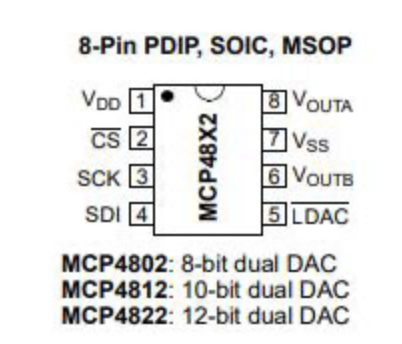
MCP4822 DAC Pinout
The Nordic nRF5340 MCU was also new hardware. For this course, we used a STM32 MCU. The Nordic MCU is very different in the sense that it runs on completely different libraries and setups. For example, the Nordic MCU involves manually configuring project.conf, CMAKE and overlay files. It is extremely easy to miss a declaration and the desired peripherals would just not work. Nordic MCU also has Bluetooth LE, which is not a feature the STM32 has on board.
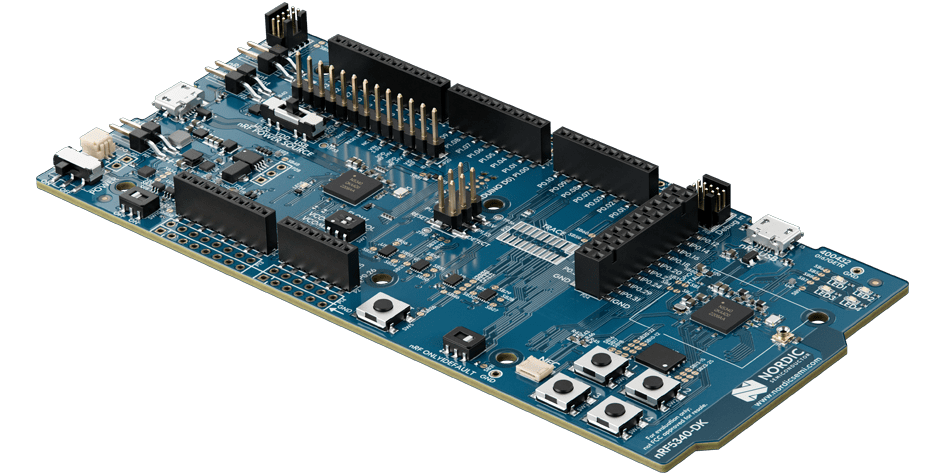
Nordic nRF5340 MCU